-
Products
- Gas analysis systems
- GAOS SENSON gas analyzers
- GAOS MS process mass spectrometry
- MaOS HiSpec ion mobility spectrometer
- MaOS AxiSpec ion mobility spectrometer
- Applications
- News
- Events
- About us
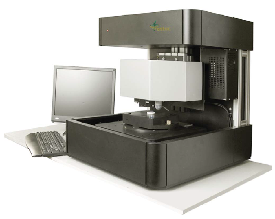
XROS MF30 – laboratory x-ray microscope-microprobe for studies of the objects by the methods of the optical microscopy, radiography, local element XRF microanalysis with possibility of the element mapping.
Using a microscope, a sample of up to 400 mm in size along the Y axis and of unlimited size along the X axis (max. scan area 150×150 mm; in the case of a larger area, the scanned areas can be stitched) and up to 105 mm high can be performed.
An overview video camera and two optical microscopes with magnification up to 200 times are using for accurate determination of the scanning area.
The central optical microscope with automated sharpness adjustment is combined with the axis of the microprobe (axis of the x-ray beam).
Local X-ray fluorescence microanalysis with the possibility of elemental mapping and X-ray studies can be carried out both separately and simultaneously.
Sample positioning accuracy is 10 microns.
The minimum diameter of the x-ray probe is 30 µm.
The range of simultaneously measured elements from 11Na to 92U.
| Scanning interval | 800 µm |
| Speed | 800 µm/s |
| Measurement time | 100 ms |
| Voltage | 40 kV |
| Current | 2 000 µA |
| X-ray tube | Mo anode |
| Atmosphere | air |
According to IЕС 62321-3-1-201 it is necessary to monitor the content of heavy metals in printed circuit boards. The document describes the screening analysis of five substances, specifically lead (Pb), mercury (Hg), cadmium (Cd), total chromium (Cr) and total bromine (Br) in uniform materials found in electrotechnical products, using the analytical technique of X-ray fluorescence (XRF) spectrometry. We apply microscope-microprobe XROS MF30 for analysis of printed circuit board to map elements.
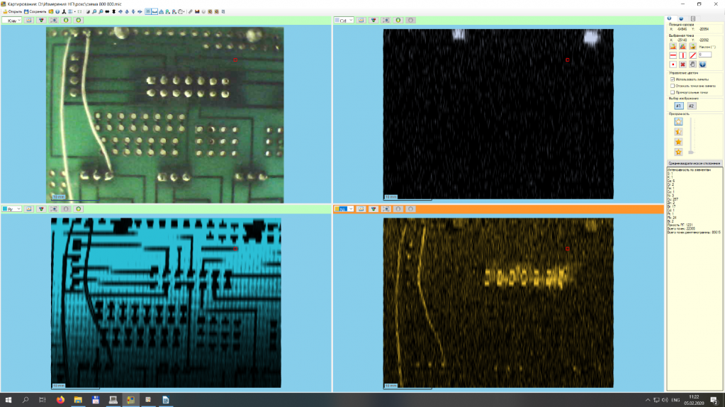
Fig. 1. The figure of the analyzed area as well as cadmium, bromine, and nickel intensity distribution map
Fig. 1 contains the image of the analyzed PCB area. The board has a coating with bromine, which is visible on the bromine intensity distribution map. There are two screws on the PCB upper part. It contains significant content of cadmium and chrome trace elements (Fig. 2).
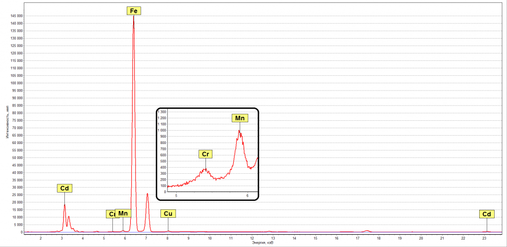
Fig. 2. Screw spectrum
One of the most important elements for monitoring is lead. As per IЕС 62321-3-1-201 it is necessary to control its content in solder alloy and other PCB elements. On the lead, tin, copper, and bismuth intensity distribution chart (Fig. 3) it is clear, that the images are not identical, which means that lead is present in various compounds. Contacts were brazed with solder, containing tin and lead. Moreover, circuit tracks also contain lead. There are two types of tracks: lead-bismuth and lead-copper ones. The measurements (100 sec. each) in additional points of the PCB were performed to improve statistical data. The spectra are on Fig. 4. The content of the elements was calculated by the fundamental parameter method (Table 1).
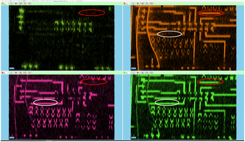
Fig. 3. Tin, copper, bismuth and lead intensity distribution maps. The Lead-copper track is emphasized by red color. Lead and bismuth track - by white color
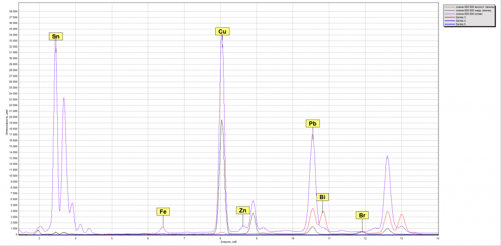
Fig. 4. The spectra of different areas of PCB: purple – solder alloy on contacts, red – lead-bismuth tracks, black – lead-copper tracks
Table 1. The results of fundamental parameter analysis (the sum of concentrations of visible elements is normalized by 100 %)
|
Object |
Sn |
Pb |
Bi |
Br |
Cr |
Cd |
Fe |
Ni |
Cu |
Zn |
Au |
Cl |
K |
Ca |
Co |
Mn |
|
Copper-lead track |
21.1 |
16.1 |
- |
2.4 |
- |
- |
0.46 |
- |
59.8 |
- |
- |
- |
- |
- |
- |
0.26 |
|
Lead-bismuth track |
17.6 |
30.9 |
48.9 |
1.26 |
0.17 |
- |
0.28 |
- |
0.69 |
- |
- |
- |
- |
- |
- |
0.19 |
|
Tin |
88.3 |
5.6 |
0.21 |
- |
- |
- |
0.22 |
- |
5.5 |
0.14 |
- |
- |
- |
- |
- |
- |
|
Screw |
- |
- |
- |
- |
0.05 |
59.7 |
39.9 |
- |
- |
0.13 |
- |
- |
- |
- |
- |
0.17 |
|
Background* |
- |
- |
- |
93.1 |
- |
- |
1.85 |
- |
2.62 |
0.62 |
- |
- |
- |
- |
- |
1.79 |
|
Wire |
- |
- |
- |
2.9 |
- |
- |
- |
- |
97.1 |
- |
- |
- |
- |
- |
- |
- |
|
Nickel spot |
0.45 |
- |
- |
- |
- |
- |
0.35 |
68.2 |
24.0 |
5.5 |
0.86 |
0.25 |
0.24 |
0.18 |
0.08 |
- |
* Light elements, which are not detectable by microscope are not considered, therefore the concentration of bromine in plastic PCB contains significant errors
The analysis demonstrated the presence of traces of lead, chrome, cadmium, bromine in the PCB. These elements should be monitored according to IЕС 62321-3-1-201. It was also determined their distribution through PCB. Semiquantitative analysis was done by the fundamental parameter method.
Microscope-microprobe XROS MF30 allows analyzing PCB by IЕС 62321-3-1-201 with an element distribution map.