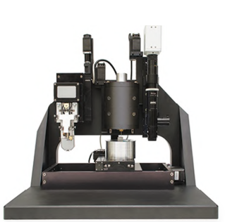
The technologies underlying NIOS nanomechanical instruments have been developed by Russian materials scientists and engineers since 1995. All technical solutions employed on NIOS instruments are protected by patents under the Russian Federation.
The modular design of the NIOS series allows end-users to configure a nanomechanical tester specifically for their needs and requirements. Configurations of NIOS nanomechanical tester can consist of the following modules:
- Wide-range nanoindenter
- Optical Microscope
- Atomic Force Microscope
- Scanning nanomechanical tester
- Electrical Properties Measurement
- Lateral Force Sensor
- In-situ Topography Imaging
- Heating Stage
NIOS Advanced is the flagship model that implements more than 30 different measuring techniques covering all types of physical and mechanical properties measurements at the submicron and nanometer scale.
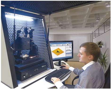
With NIOS control software a high degree of automated measurements can be achieved allowing the end-user to configure any set of measurement recipes to be performed without operator intervention. This feature is particularly useful for the technical control of the quality of the materials. With this added functionality, NIOS can be used for research work as well as for industrial applications.
Application Areas
Unique features of NIOS allows the instrument to be used in traditional nanomechanical testing and in areas that require SPM techniques to get mechanical properties characterization.
Materials science. Scientific research and engineering:
- Nanophase and composite materials
- Ultra dispersive hard alloys
- New hard and superhard materials
- Structural nanomaterials: alloys, composites, ceramics
- Thin films and coatings
- Carbon nanomaterials and fibers
Energy:
- Nanostructured materials for nuclear energy
- Coatings for turbine blades
Instrumentation engineering:
- New semiconductor materials
- Optical components
- Micro- and nanoelectromechanical systems (MEMS and NEMS)
- MicroChannel plate for night vision devices
- Storage devices (i.e., Hard Disk Drive)
- Nanolithography
Medicine:
- New materials in dentistry
- Nanostructured materials implants
- Bioactive coatings
- Stents
Industry: automobile, aircraft construction; space research and mechanical engineering
- New structural and functional nanomaterials
- Wear-resistant coatings for machine elements
- Coatings for cutting tools
- Carbide tools quality control
- Diamonds and diamond powders
Metrology:
- Linear dimension measurements at the nanometer scale using 3-axis laser interferometry
Packaging:
- Protective coatings for plastic products
-
Glass and metal decorative and functional coatings
Education:
- Nanoindentation & Scanning Probe Microscopy laboratory courses
- Advanced research
|
All NIOS measurements are performed in an open environment (i.e. without the use of special vacuum or heat treatment).
NIOS instruments are designed with features and functionalities that allow its use for research and industrial applications.
|
Measurement modes and methods
Mechanical properties:
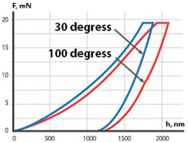
- Instrumented indentation in accordance with ISO 14577
- Vickers microhardness measurements
- Sclerometric tests (hardness measurement by scratching) with constant or variable load
- Force spectroscopy
- Mechanical nanolithography
- Beams and membranes stiffness measurements
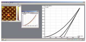
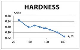
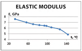
- Hardness and elastic modulus dependency of the indentation depth
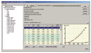
- Automated mapping of two- and three-dimensional hardness and elastic modulus distribution over the surface within the area of 50x50 mm
- Adhesion characterization by the scratch test
- Measurements in liquids
Nanotribology:
- Cyclic surface abrasion with an applied load
- Nanotribological tests with grease on an investigated surface
Optical microscopy:
- Selection of the field for nanomechanical testing
- Objects sizes measurements and high-precision positioning
In-situ modes of scanning:
- Surface profiles on a linear basis up to 50 mm measurements
- Relief semi-contact dynamic scanning by the diamond indenter
Local electrical properties:
- Current-voltage characteristics measurements with a controlled load or an indentation depth
- Current Spreading measurements in the nanomechanical tests
Atomic Force Microscopy:
- Contact Atomic Force Microscopy (AFM)
-
Vibrational (semi-contact) Atomic Force Microscopy (VAFM)
-
Scanning Tunneling Microscopy (STM)
-
High magnetic fields microscopy (M-AFM)
-
Electrical conductivity and electrical potential microscopy (E-AFM)
-
Force Modulation (FM-AFM)
-
Lateral Force Microscopy (LF-AFM)
-
Viscosity Force Microscopy (V-AFM)
-
Adhesive Atomic Force Microscopy (AD-AFM)
-
Lithography Mode (AFM-LIT)
-
Hardness measurements according to residual imprint
-
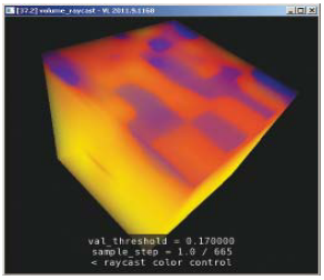
The extended set of roughness parameters calculation for two- and three-dimensional images of the surface relief in accordance with international standards
-
ISO 3274, ISO 4287, ISO 13565 and ISO 16610
Measured characteristics
- Hardness from imprint (microhardness)
- Hardness from instrumented indentation (nano hardness)
- Elastic modulus (reduced young's modulus)
- Coefficient of elastic recovery
- Adhesion
- Coating thickness
- Mechanical properties mapping
- Mechanical properties vs depth
- Mechanical properties vs three coordinates (tomography)
- Microstructures stiffness and displacement
-
Fracture resistance
-
Durability
-
Linear wear intensity
-
Coefficient of friction
-
Lateral force during scratching
-
Surface topography
-
Roughness parameters
-
Local voltage characteristics
-
Electrical resistivity
NIOS software
- Automatic measurements by instrumented indentation, sclerometry, force spectroscopy, AFM and SPM methods
- Parameters setting using an optical microscope or surface relief image obtained with AFM or SPM method
- High performance of experimental nanoindentation data (using new parallel calculations) batch processing
- Flexible setting of the indentation reports
- Macro-commands language allows performing a random sequence of the measurements in the automatic mode
- A wide set of mathematical functions allowing to perform a variety of the conversions, plotting of the spectra, filtering, obtaining two- and three-dimensional data and approximation of the curves
- Two- and three-dimensional mapping of hardness and elastic modulus distribution versus coordinates
- Measured mechanical properties and the roughness parameters calculation in accordance with appropriate standards