-
Products
- Gas analysis systems
- GAOS SENSON gas analyzers
- GAOS MS process mass spectrometry
- MaOS HiSpec ion mobility spectrometer
- MaOS AxiSpec ion mobility spectrometer
- Applications
- News
- Events
- About us
The indenter working as an optical objective
The new approach of nanomechanical testers design is realized in NIOS with a transparent diamond tip.
This option allows one to obtain a full optical image of the investigated area of the sample surface, including video imaging directly during measurements by applying the indentation and scratching methods.
An optical image of the fused silica surface during scratching can be seen in the video. Three black lines correspond to the ridges of a diamond tip, the tip’s end is situated on their intersection. The second half of the video shows the process of cracking the surface. At some point in the load the stress is accumulated at a significant degree, and it can not be released through the plastic deformation. Thus surface starts cracking. Making time-related correspondence between the force load and probe’s movement on the video, one can find the critical force, which starts changes of the type of deformation.
Nanomechanical tester with transparent indenter allows:
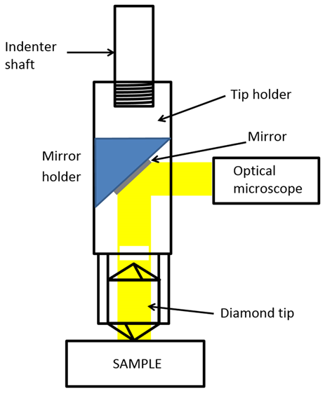 |
The construction of NIOS with a transparent indenter consists of a two-sided centrally symmetric Berkovich pyramid, which is pressed into a brass holder.
We proposed the new indenter’s tip geometry which is cut from both sides – from the working edge and from the opposite edge. Thus, the indenter works as a lens with 0 optical power. And parallel beam stays parallel after passing through such indenter. This allows us to look through the indenter tip and optically see what happens underneath the tip during the indentation and during the mechanical testing.
A holder is connected to a mirror mounting block, installed on the working rod of the device.
In our company, we have the facilities for growing diamond crystals and for cutting diamond crystals and for analysis of its geometry and structure. So, we produce such indenters by ourselves using our patented technology. We control the process all the way starting from X-ray topography of raw crystals and up to Atomic Force Microscopy of indenters apex. It lets us keep the quality of diamond tips at a very high level. |
|
The microscope is equipped with a digital camera to register images.
|
 |
The video demonstrates the optical image of the TGZ2 test grating for AFM scanners calibration under the apex of a diamond tip, while it moves along the surface. The lateral resolution of the optical image is 5 μm.
Using such an image one can choose directly the point of interest for further measurements and scratch. No need for switching the sample’s positions between the indenter and the optical microscope modules provides a more accurate tip’s positioning.
Also one may notice that the indenter doesn’t hurt the optical image. This is a unique feature of our NIOS Nanomechanical Tester, which no one other has so far.
 |
 |
|
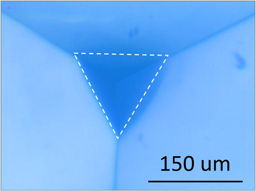
a) The image at peak load, Amax = 9230 sq.um |
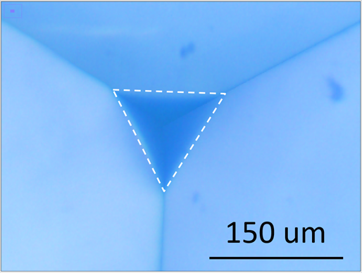
b) The image after complete unloading, Ares = 7230 sq.um
|
The images, that are presented above, allow comparing the areas of the obtained indentations and, hence, the material hardness with the corresponding values that were obtained by the instrumented-indentation method.
This model experiment was carried out on a material with known elastic properties (polycarbonate with the values of the Young modulus and Poisson ratio, respectively, E = 2.9 GPa, = 0.37). After calculation of the contact area Ac from the video image, further, we can calculate the hardness H based on the measured values of loading force Fmax and contact stiffness S.
The sample investigated is the welding separation border between two metal alloys. The video shows changes in the shape of scratch when the probe moves across the separation border. Using the image scaled, one can calculate the thickness of the scratch for both metals. This information can be used in addition to scratch normal load 300 mN, measured by the indenter itself.
All materials show different behavior during scratching. Transparent video indenter allows us to visualize it just during the experiment. On the videos above one may see scratching of 1 um MoC coating, deposited on silicon (upper) and steel (lower).
Silicon surface is brittle, it tends to crack after some critical load. One may observe its cracking process during loading, save images of the exact shape of the defects appearing, and analyze them later. The steel surface is ductile, and scratch looks to be uniform in the range of loads from 5 to 200 mN.
Later, using a combination of video images and surface profiles, obtained during the indentation process, we can estimate some geometric parameters like an area of delamination, radius, and the opening angle of scratch arcs.
The transparent indenter also can be used as an optical objective for Raman spectroscopy.
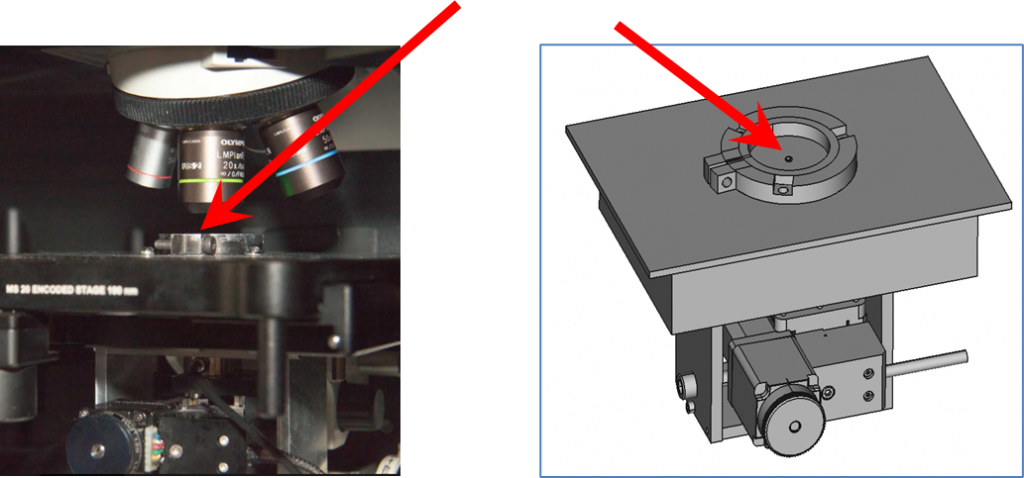
Our engineers developed a special load application unit, capable of being used with the standard laboratory Raman Spectrometer. This unit consists of a linear translation stage with a stepper motor, tenso-resistive load cell, sample holder, and a housing.
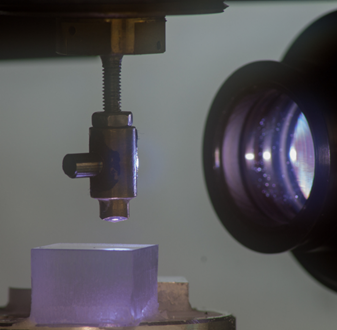
A drawing and a photo of this unit in the confocal microscope are shown below. Raman spectra can be measured simultaneously with loading and unloading directly through the transparent indenter.
|
Indenter is fixed here |
 |
A silicon sample with (100) surface orientation was investigated for the demonstration of simultaneous loading and Raman spectra measurements. The spectra were collected through the 20x objective at loads of 3 N, 10 N, 20 N, 30 N, 40 N and 50 N during loading and unloading process. During the loading Si-I peak, which is observed for the undeformed sample, it became skewed and moved to higher frequencies.
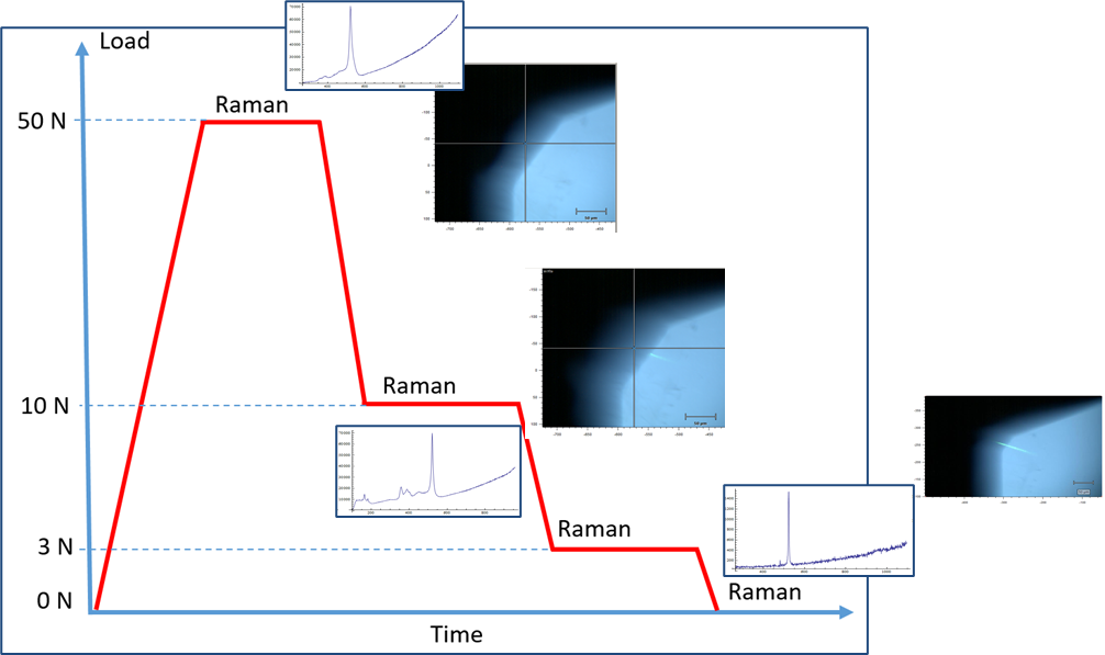
An image below shows Raman spectra, obtained during and after unloading part of the indentation. Observation of Raman spectra under pressure may add some interesting data. For example, Si-II-marked peak, which is visible only at 50 N – curve, can be attributed to Si-II phase. This phase exists only in the loaded state and simultaneous indentation + Raman makes it possible to be detected.
As the load decreases from 50 N to 0 N one can observe transformation of spectra, which corresponds to appearance of new Si phases. Slow decompression at room temperature leads to Si-II -> Si-XII deformation, at the relatively low pressure of 2 GPa Si-XII -> Si-III transition occurs.
All such researches in the past demanded first to make indents, and then to find them to measure Raman spectra. Our development allows us to obtain all information about Raman spectra of the surface under load in-situ.|
|
|
Raman shift, 1/cm |