Quasistation instrumented indentation testing is the basic function of NIOS devices. The algorithm is based on measuring and analysis of indentation load-displacement data. This technique underlies the international standard of hardness testing ISO 14577. The typical experimental curve of load (P) versus depth (h) contains loading and unloading parts.
Typical load-displacement curve (a) and diagram of the indenter and the surface contact (b). The hardness and elastic modulus calculation parameters are presented in the figure.
Reduced elastic modulus Er is calculated from the initial slope of the unloading curve S and contact area Ac. The contact area is defined by the dependency of the pre-calibrated area Ac (hc) on contact depth hc, which is in turn calculated from maximum indentation depth hmax and unloading slope S. Additional parameter β accounts for the non-axis symmetry of the indenter tip. Reduced Young's modulus of the sample is calculated from Er according to indenter tip material properties and sample's Poisson ration.
Multiphase materials research
Multiphase materials properties study involves precise indenter positioning in the specified areas of the surface corresponding to the individual components. NIOS nanomechanical testers combine the functions of a scanning probe microscope and a hardness tester.
The device allows to obtain three-dimensional surface topography image of a multiphase sample, and then specify measurement location with a connection to the resulting image.
Positioning accuracy of the indenter relative to the surface at measurements is about 10 nm in the XY plane.
Example: D16 aluminum alloy sample.
Topography images of the same surface area before and after a series of measurements.
D16 aluminum alloy. Surface topography: before indentation (a), after indentation (b), a load-displacement curve for phases with different properties (c).
Tomograms of mechanical properties
Basic instrumented indentation test (ISO 14577) contains a single loading-unloading cycle and thus gives hardness and elastic modulus that correspond to one depth. NIOS testers can perform an indentation with partial unloading (PUL): at a given position on the surface, tip penetrates the sample, partially goes back and penetrates deeper again. Such kind of penetration repeated within multiple cycles gives a possibility to profile mechanical properties along with the depth.
Tests that allow profiling mechanical properties (PUL or DMA) along depth can be arranged with the grid that partially covers sample area, which gives the opportunity to map mechanical properties along three axes (X, Y & Z). Corresponding data are used to construct tomograms of elastic modulus and hardness. Maximum surface area for the tomogram can be up to 10 cm x 10 cm, maximum depth is limited by sample properties but cannot be bigger than 200 um.
Hardness measurements by the residual indentation imprint
NIOS nanomechanical tester provides hardness testing by the residual imprint method (ISO 6507-1:2005). In contrast to traditional micro-hardness testers, the imprint dimensions measurement is made in scanning probe microscopy (SPM) mode. Indentation and corresponding surface topography imaging are performed using the same probe sensor and the same tip. Three-sided Berkovich diamond pyramid is used as an indenter, tip apex angle is 140° and the radius of curvature is ~50 nm. According to the residual imprint method, the hardness is defined as the ratio of the maximum applied load to the area of the residual imprint, measured from the SPM image.
In case of the plastic pile-ups formation on the residual imprint perimeter, a three-dimensional image allows to determine the pile-ups area and take it into account when calculating the hardness value. NIOS software allows automated measurement
of indentation area and takes the pile-up effect into account.
Indentation imprint on the titanium surface 99% (a); example of automated area calculation (b); indentation imprint profile (c).
Scratch hardness testing
Determination of hardness by scratching implies making a scratch on the sample surface and measuring its width. You can use different NIOS modules to measure this value: optical microscope, AFM or scanning nanomechanical tester which scans the surface in SPM mode and makes the scratches with the same probe.
Similarly to instrumented indentation scratch measurements require pre-calibrated function for tip shape. This is achieved by measuring widths b of the scratches, performed on the surface of the reference sample with the different (increasing) loads. For the given load P hardness H is inversely proportional to the scratch width b, according to the given below equation. Ideal pyramid tip requires single coefficient k for calibration.
Despite scratching does not give an information about the elastic modulus the method has its own advantages. In contrast to the instrumented indentation determination of scratch hardness makes an account for the pile-up effect and, what is of particular importance for the thin and rough films, is less sensitive for roughness.
Cross-section profile examples of the residual scratch groove for fused quartz (solid line) and aluminum (dashed line). Arrows indicate the width of contact area between the indenter and the material during the scratch test.
Comparative hardness tests
Material
P, mN,
normal load
Rscrxy,>% creep
recovery of
scratch width
Rscrz,%
creep recovery of
scratch depth
RNIz,%
creep recovery
of indentation
depth
Hscr, GPa
scratch hardness
HNI, GPa
nanoindentation
hardness
Fused Quartz
20
15
47
46
Ref.
10,1
Glass
20
16
49
44
9,7
9,3
Bi2Te5
7,6
13
23
30
2,6
2,8
Ni
15
10
15
13
4,7
4,8
Al
1,7
1
3,2
4,2
0,5
0,6
Mechanical properties measurements for materials and thin films (hardness, adhesion, thickness) by a variable load scratch test
Thin films are used extensively as protective and wear resistant coatings for a wide range of objects. Accurate mechanical properties measurements of these films without the substrate influence is an important task in the modern quality control systems. NIOS nanomechanical testers allow films hardness measuring by different methods for a wide range of thicknesses. Instrumented indentation is the most common method of measuring physical and mechanical properties of thin films. However, there are several factors that lead to methodological errors in this measurement method. The most critical are surface roughness, residual stresses and so-called “substrate effect” (for the film-substrate system the response of the material depends both on the film properties and the substrate properties). The scratch test method (scratching and scratches profile analysis) has several advantages over indentation methods for measuring the films hardness at the nanoscale. Direct SPM observation of the residual scratch trace allows to minimize the influence of the dominant elastic deformation which is typical for the indentation methods. Scratching at variable load makes it possible to define several film parameters in a single measurement procedure: elastic interaction area, limiting load at which the plastic deformation starts (there is a visible trace on the surface), separation and delamination of the film.
Scratch with a linear zoom of a load on a surface of a diamond-like film on a silicon substrate.
Elastic modulus measurements by force spectroscopy
NIOS nanomechanical testers are capable of measuring the quantitative value of the elastic modulus. This method involves probe sensor oscillating simultaneously with loading. The oscillation amplitude is less than 10 nm, frequency is around 10 kHz. When the diamond indenter contacts the surface, the frequency increases with increasing load.
According to the analytical description based on the Hertz model, the slope of the frequency dependence versus probe displacement (approach-retraction curve) is proportional to the elastic modulus of the material.
Prior to the test the device is calibrated on reference materials with known elastic modulus values. The resulting elastic modulus value is evaluated as a proportion between approach-retraction curves slopes and reference elastic modulus. This method is nondestructive.
The material layer involved in the test can be as small as 100 nm. This makes it possible to measure thin films elastic modulus without substrate influence. The comparative measurements on different materials showed accurate elastic modulus values in the wide range.
Approach-retraction curve measurement schema (a); the slope of Δf curve characterizes the elastic modulus of the material (b).
Wear resistance measurements
Wear resistance testing of coatings is implemented in the NIOS devices. The test principle is based on specified indenter movement while keeping the constant normal load and recording the normal displacement of the indenter. Indenter will deepen inside the surface due to material wear. After some time the indenter will break the coating and reach the substrate, which is indicated by change in the diagram slope.
In case of standard triangular tips being used indenter moves in a "square” path taking account of the indenter asymmetry. In case of spherical indenters made of different materials being used reciprocating indenter movement is realized.
"Square” tests by a pyramidal diamond indenter (a); wear test results for a spherical sapphire indenter (b). Overlaid graph axes label: horizontal axis T indicates time in seconds, vertical axis Z indicates average penetration into the sample surface.
Simultaneous surface topography mapping and mechanical properties distribution
Semi-contact surface scanning and quasi-static mechanical testing are two basic options of NIOS scanning nanomechanical tester. Measurement head (which uses a piezo ceramic probe working in self-oscillation circuit) construction allows to simultaneously measure not only surface topography but characterizes its mechanical properties as well.
Such kind of additional information that can be recorded during any surface scanning provides rapid mechanical characterization. The resolution is about 10 nm in XY plane and about 1 nm along Z-axis.
Composite carbon fibers. Surface topography (a ); stiffness map (b)
Dynamic hardness measurement
Dynamic hardness measurement is implemented in NIOS devices. This method is based on simultaneous processing of oscillating and direct movement of the indenter. This method is less influenced by surface roughness compared with quasistatic nanoindentation. However, it requires information about the elastic modulus value. The final equation used for such kind of measurements is the following:
where F and Δf - force and resonance frequency shift, both are measured during the scanning, f0, and k - probe resonance frequency and dynamic stiffness. Last two parameters are determined during the calibration procedure and considered to be constant in future measurements. This equation leads to H/E2 determination (the value of H or E if the other one is known) as a function of the depth or coordinates of the surface.
Hardness map of hard fiberglass in a soft matrix (a) and fused silica hardness versus depth (b). In both cases, elastic modulus was taken from the other sources.
Surface profiling with the mechanical tester module
Scanning nanomechanical tester and wide range indenter modules can measure surface profiles. The maximum length of measurement makes up to 10 mm and 100 mm correspondingly. The maximum measurable slope for the standard indentation tip (Berkovich pyramid) is 10 degrees, optional tips are available. The horizontal resolution depends on the type of the module used, scanning speed and has a limit of 10 nm in a horizontal direction and 10 nm in a vertical direction. All profiles are obtained in semi-contact scanning mode.
A sleeve (a) and the corresponding profile of cylindrical surface (b).
Application:
Surface roughness measurement
Part's shape control
Small objects location
Surfaces flatness
Mechanical Nanolithography
NIOS devices provide sample opportunities for precise mechanical micromachining and nanolithography. The diamond tip can cut almost all known materials. By controlling the load during the cutting process with a resolution of 10 pN, one can steadily get scratches with 100 nm width and a several nanometers depth. The maximum scratch depth reaches several microns.
By using high-precision piezoceramic nanopositioners and mechanical linear translation stages, the diamond tip positioning accuracy reaches 10 nm in a 100 x 100 pm area and about 1 pm in a 100 x 100 mm area.
The result of a surface micro treatment can be controlled by the same diamond tip via scanning in the SPM mode or via digital optical microscope.
The mechanical nanolithography mode can be used to create regular structures on the surface, remove oxide films, clean the coatings in selected areas and adjust the microelectronics and micromechanical systems (MEMS) elements’ geometry.
Golden coating removed from a diamond substrate (a); inscription made by scratching the fused silica surface; scratch profile (b).
Micromechanical stiffness measurements
NIOS devices are capable to control stiffness of different objects: cutting tools, beams, MEMS and NEMS beams and membranes. The value is calculated according to the force-displacement diagram, i.e. the same curve as it is used in the instrumented indentation analysis. Different modes of loading are possible, including multiple loading-unloading mode, which allows to get average stiffness value as well as to determine a number of cycles to failure.
NIOS systems allow to determine the measurement location by in-situ SPM pre-scanning (scanning nanomechanical tester module) or with the help of optical microscope that works with the wide range indenter module.
Stiffness measurement of the cutting tool (a). Membrane properties measurement scheme (b). Loading-unloading curve (c): 1 - membrane bending (stiffness measurement); 2 - contact with the substrate.
Surface electrical properties measurements
Boron-doped diamond tip allows conducting electrical properties analysis: measure sample’s specific resistivity, current spreading during the surface scanning or indentation. Measurement of volt-ampere characteristics with the given load or penetration depth is also possible. Current spreading map is measured with the constant voltage bias between the tip and the sample. Measurement of current spreading at the different surface locations allows to identify location with the different conductivity and to compare them with the surface structure and inclusions.
Measurement of the current spreading during the indentation allows investigating material's heterogeneity along its depth, control coating thickness and study phase transitions in semiconductors under pressure. Simultaneous processing of force and current vs depth dependencies allows specific electrical resistivity calculating. Measurement of volt-ampere characteristics is conducted in the contact with the material with the force ranging from 0.1 mN up to 100 mN. Voltage range is ±10V, current range is ±30 µA, current measurement resolution is better than 10 pA.
Surface's microstructure of AlCuCo alloy. Map of conductivity (a). Areas with different colors correspond to different crystal structures of the alloy. Electron microscope image (b).
Сrack resistance measurements
As a measure of resistance to materials brittle fracture it’s common to use critical coefficient intensity of stress Kc - fracture toughness. Fracture toughness is one of the most important coating parameter which describes its wear resistance. Common method of brittleness study is to destroy material by pushing the indenter into it, gaining fractures of different sizes.
Material rack resistance can be defined by scratching. In this case Kc value is connected with a critical scratch width. After achieving this width elastic deformation transforms to brittleness deformation. There are more than 30 ways to calculate Kc using values of applied load and length of the fracture. Ways to define Kc for thin coatings are being researched very intensively. Indentation at a small depth produces radial or half-penny fractures along the ribs of an indenter With increasing load coating delaminates from a substrate. Canal cracks leading to destruction of the substrate and spiral cracks within coating detachment from the substrate are occurred.
NIOS devices have several methods of thin coatings crack resistance measurement based on scratching and instrumented indentation.
Scheme of coating destruction with cracks formation.
Metrological support of linear dimensional measurements at the nanoscale
Metrological characteristics of SPMs and metrological support of linear dimensional measurement at nanoscale are very important for equipment dealing with technological and certification tasks and for nanotechnology products control. The interferometer module of NIOS is designed as a compact plug-in instrument for the real time measurements. A source of radiation is a single-frequency stabilized He-Ne laser (power 1 mW, wavelength 632,991084 nm, relative instability of optical frequency no more than 3x10⁻⁹ during 8-hour work).
Metrological characteristics inspection was conducted with linear measures TGZ1, TGZ2, TGZ3 calibrated by SPM in PTB (Germany). For all three measurements results are included in 95% confidence interval estimated by PTB equipment. Obtained results certify the designed device as an etalon of linear dimensional measurements at nanoscale that allows to support a traceability of linear dimensional measurements of nanostructures by scanning probe microscopy methods.
Measure
Step height, nm
NIOS
PTB (Germany)
TGZ1
18.1±0.2
18.4±1.0
TGZ2
100.0±0.4
101.1±1.6
TGS3
488.0±0.9
489.0±1.8
TGZ1 measure profile (21,4 nm) measured by NIOS
Mechanical testing of micro-objects
A high accuracy of mutual positioning of an indenter and a sample and using indenters with different geometry allow to implement in NIOS devices mechanical properties testing of micro-objects. In particular there is a method of mechanical durability determination of polyelectrolyte microcapsules produced with LBL technology based on a consecutive adsorption of poly-cations and poly-anions on a charged substrate.
Characteristic diameter of objects can be from several to hundreds microns. Accurate geometry of the object is defined by using an optical microscope. Diamond flat stamp with a specified diameter is used as a tip. The load after which capsule destruction is occurring is defined from a registered load-displacement curve. Mechanical durability is defined from ratio of the load to the capsule diameter.
This method is widely used for biological objects, pieces of dye used in the toner and during testing of particulate abrasive materials.
Object positioning by microscope (a), micrograph of a diamond flat stamp indenter (b), load versus displacement registered while capsule compression (c).
Mechanical properties profiling
Due to automatization of conducting series of measurements along specified line or area the mapping and profiling methods of mechanical properties are implemented in the NIOS devices.
This method is important for studying object which structure has inhomogeneous mechanical properties. For example, a golf ball consists of a core and a several layers with different properties with thickness range from microns to millimeters. Measurement can be conducted in the open air and in liquid.
NIOS software allows automatic measuring, profiling and mapping of hardness and elastic modulus distribution over the area from several dozens microns to 100 millimeters with specified step between points.
Properties of different layers in the golf ball
Parameter \ area
Core
Inner protective layer
Polyurethane layer
Inner ink layer
Outer ink layer
Thickness, um
-
1100
800
12
15
Hardness, MPa
15
45
15
10
5
Elastic modulus, MPa
10
600
150
80
60
Optical images of the sample and hardness profile. Core, inner layer, polyurethane layer (a), (b); polyurethane layer and two ink layers (c), (d).
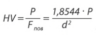
Vickers microhardness measurements
NIOS nanomechanical tester provides microhardness measurements over the residual indent image in accordance with ISO 6507. This method is used in usual micro-hardness testers.
Four-side Vickers pyramid is used as an indenter (the angle between opposite sides is 136°). Measurements are provided with optical micro-images. Hardness HV is calculated as a maximum of an applied to indenter load divided to an area of residual imprint measured with its image:
d - medium length of a quadrangular imprint (mm), P - maximum load (kgf).
Vickers hardness is one of the commonly used methods of a hardness measurement. Combination of that and other methods of a nanohardness measurement allows to compare and define hardness at different scales.
Imprint in a standard hardness measure. Load is 200g. Hardness is 270 HV 0.2.
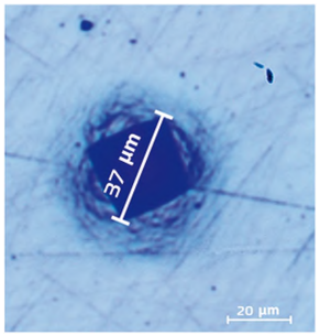
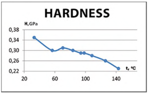
Measurement of temperature dependence of mechanical properties
The heating stage with a heating control is applied for materials mechanical properties measurements at high temperature. The heating stage allows to heat a sample up to 400 °C and conduct all types of mechanical tests implemented in NIOS. Maintaining accuracy of a given temperature is 1 °C.
Test results include hardness, elastic modulus, creep recovery, crack resistance, wear resistance and other characteristics at a specified temperature.
Typical sample dimensions for temperature testing in NIOS are 25x25x10 mm.
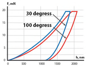
Hardness and elastic modulus versus temperature graphs of polymethylmethacrylate (PMMA) at 140°C
Hardness and elastic modulus versus temperature graph of PMMA. Load-displacement curve at 30°C and 100°C, measured on a PMMA sample
Dynamic measurement analysis
NIOS supports measurements of mechanical properties by Dynamic Mechanical Analysis.
According to the method oscillating force is imposed over the linear increasing load and applied to the surface while corresponding in-phase and 90 degrees out of phase components are measured.
Obtained data is used for the calculation of real and imaginary components of signal, which in turn are used for the calculation of storage and loss elastic moduli E’ and E". Hardness value is calculated as well.
Supported range of frequencies goes up to 50 Hz, oscillation without the analysis may be performed up to 250 Hz.
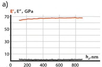
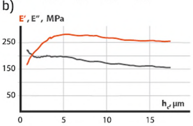
Measurement of elastic modulus E' and loss modulus E" of a fused silica (a); bitumen (b)